Warning : update in progress
In the beginning, YASEP was called "the VSP", which stood for "Very Simple Processor", but "Very Silly Processor" fits well too. Today, it is renamed to YASEP ("Yet Another Small Embedded Processor"), though some original documents keep the old name for historical reasons.
YASEP is a microcontroller core with 16/32-bit instructions and 16 registers, with emphasis on simplicity, small size and memory bandwidth. Originally designed as a 32-bit architecture, it now also available as a mostly-identical scaled-down 16-bit version.
It is also an experimental core that uses very unusual techniques. The YASEP introduces and tests new methods in many domains : ISA design methodology, architecture, software development environment...
Being a microcontroller, there is no need for sophisticated instructions such as multiply/divide. The YASEP's intended job is (hardware and environment) management : it moves data around a SoC, keeping other specialised processing blocks fed with data, answering user requests through a keyboard/LCD screen interface, and overseeing the system's health (power management and system configuration / hotswap).
So it's an embedded core. The initial target speed was in the range of 10M instructions per second with an old Silicon process, but 25MIPS seems possible in an Actel ProASIC3 FPGA. It was not intended to be pipelined but feature creep is slowly taking over. It's a rather simple core, until you look at the memory interface, which (like F-CPU's FC0) plays a critical role in the system's efficiency.
When there is no need for horsepower, implementing a complex stuff is a waste of resources, time, money, efforts, silicon, energy...
So it naturally takes the barebone RISC route, with a very clean instruction format. The main idea behind YASEP was that it further simplified this by merging some of the instruction fetch mechanism into the data fetch machinery (or is it the reverse ???). Both are software controlled and this spares more instructions.
This comes at some price : it is furiously uncommon and might create new issues when programming, such as register usage through function calls. But you don't want to use C with YASEP (unless the compiler is designed specifically for this architecture).
However, the design shines with its simplicity and low resource consumption, as you can see from the draft below. It has evolved a bit, since, but not radically.
Because I needed something like this at one time (around the end of 2002). Well, now I don't need it anymore for a "real industrial project" but the idea sounded so coooool and there was no reason to stop, even if the original project was cancelled.
And because F-CPU development is almost stalled (huh .....). It is a good way to develop something fun and helpful later for FC0, which has many implementation problems. I'll probably be able to solve them once I've put YASEP together.
Also, it is probably one of those solutions waiting for a problem : YASEP has found some support lately (small but encouraging).
Like other projects, you may be interested because it is fun, it is instructive and contributes to the Free Hardware movement.
Another reason is that it is weird and you may want to scratch itches here and there. Help yourself.
A better reason : you may need something like that. ARM's license costs may annoy you, and other "free" cores don't suit your needs. In fact, most fall in the same category of the 16/32-bit small processors for low power and low-resource applications. But YASEP has an edge with memory bandwidth.
Finally, because I will reinvest all the efforts from YASEP into F-CPU/FC0, you may want to see how F-CPU works (well, roughly) by examining a small-scale loosely related core.
The YASEP is NOT meant to be a high-performance workstation processor that run UNIX, Linux or whatever. If you need horsepower, try something else like F-CPU (when it's ready).
YASEP will use specific code generation tools that give optimal access to all the features of the architecture. This would not be possible with existing tools or environments. The assembly language is often preferred and is already well supported by the online JavaScript framework.
If you're brave enough, you can attempt to create a C compiler for YASEP, but this is a bit sarcastic. If you want to lose time, port GCC. But YASEP's architecture does not suit C nor GCC well. In fact YASEP is designed to be programmed in assembly language, which is quite simple thanks to a barebone RISC approach. YASEP is a microcontroller, after all.
One side effect of YASEP's structure is that it is quite easy to use stack-based languages, particularly FORTH, and maybe JAVA. Porting FORTH is probably the easiest entry point and the best suited environment for such a microcontroller. Everything is written mostly from scratch, there's much room for improvement and no bloat, the user had flat access to all resources...
Another "solution" is the graphic, online interactive editor/simulator that is being developped in parallel. Look at ploped or "borked", both are JavaScript based versions of GNL (http://f-cpu.seul.org/whygee/gnl/). But they are not yet ready.
The YASEP reuses some parts and concepts developped for FC0. It also inherits some common ideas developped in the 90's for other projects.
The instruction set is very orthogonal, making decoding particularly straightforward. Several opcodes may seem redundant or congruent, but eliminating them would make the decoder too complex.
More than FC0, instructions are so simple that they all take the same amount of time to complete, so there is no scheduling problem. The possible points of stall are only in the memory interface and the buffers (instruction or data not ready). Furthermore, because the core is not deeply pipelined, invalid instructions are detected and handled without complex synchronisation circuitry.
The same separation of the configuration space (the Special Registers and the GET/PUT instructions) from the memory space make YASEP and FC0 close cousins.
The YASEP reuses parts of the development methodology and tools of F-CPU. Being smaller, YASEP will fit in a cheaper FPGA, though ;-)
However, the YASEP is not designed to be scalable, fast or running Linux.
Please note that I make a distinction between the execution core and the whole YASEP "IP core" because the current analysis (as of 2007) lacks the memory interface and controller, which is quite complex. The execution core runs almost separately from the memory controller thanks to small cache buffers that are not yet designed.
Note : Since 08/2008, the first YASEP VHDL core targets FPGA so the following description may be inaccurate, particularly in the way jump instructions and memory are managed (due to hardware structure limitations). YASEP now looks more like a classic microcontroller but later, it will probably revert to the original intended memory architecture.
YASEP was designed for economy and code compactness so a mixed 16-bit and 32-bit format was chosen. Well, in fact, "compactness" does not matter that much, and extreme code compression would make the instructions too complex and difficult to decode with as few logic gates as possible, which goes against the first requirement of economy. Memory is dirt cheap today (but not access time or bandwidth), and the available bandwidth/speed ratio is still comfortable. So simplicity (and orthogonality) is more important than feature creep.
There are no 16/32-bit "modes", only a single bit in the instruction that tells the decoder how to behave. And even then, the instruction is almost identical. The only difference between 16-bit and 32-bit forms is the 16-bit immediate field (called Imm16). The rest of the instruction fits in 16 bits, including the 16/32-bit flag.
The instructions generally consist of the "immediate flag", followed by a 7-bit opcode and two 4-bit register addresses. So in the 16-bit form, the core is "2-address machine", where one address points to both one source and the destination (think x86...). In the presence of the "immediate flag", a 3rd immediate operand is provided so the 2 register addresses point to one source and one destination.
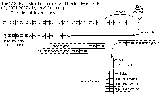
The opcode map shows that the opcodes are currently grouped into 16 groups of 8 (or less) closely related functions. Currently defined groups are :
The instructions are aligned on half-word boundaries (16-bit words). This means that the pointer to an instruction is always even (the LSB is cleared and/or ignored), whether the instruction uses 16 or 32 bits. This is a relaxation of the earlier alignment rules, because today's instruction prefetch unit could use some small FIFO. This increases code density, as well as the prefetch complexity (a bit).
The YASEP handles integers only. Depending on the datapath width, the natural data format is the 32-bit Word or the 16-bit Word, used by most operations. Some operation can also process 8-bit Bytes, as well as 16-bit Half-word in YASEP32, in the IE unit. Bit-granularity operations are provided with the ROP2 and SHL unit.
The instructions have room for 4 register address bits, or 16 registers. They can contain 16 or 32 bits depending on the datapath width. Only 4 registers are "normal" : R0, R1, R2 and R3 can contain any temporary data. The remaining registers are used for program control and memory access.
Data and Program access in memory use 10 registers, which are in fact 5 pairs. One register in the pair contains the address, and the other contains the data stored at the given address. Hence their names : A1/D1, A2/D2, A3/D3, A4/D4, A5/D5. This is quite similar to how the CDC6600 Central Processing Unit worked in the 60's :
mov 1234h A1
mov 5678h D1 ; writes the value 5678h to the address 1234h
mov 1234h A1 ; reads the contents at address 1234h into D1
add D1 R1    ; Adds the contents of the memory to R1.
The scarcity of the "normal registers" is a trade-off with the need for data pointers, stacks, jump/call/return destinations... But Data registers can also be used as "normal registers" when the auto-update is disabled and the Address register points to an unused memory location. Writes to the Data register will still trigger memory writes as a side effect, but it frees one register when memory references are not needed.
Program control takes the last 2 registers :
Instruction fetch is shared with data access. The decoder takes instructions out of one of the four first queues, leaving the two others to stacks. When the instruction stream is linear, a couple of queues are enough, so four queues are used for data moves. When the code becomes more complex, the four queues can contain pointers and instructions from several entry points in loops or functions, leaving one stack (or none) and one (or two) queue(s) for everyday data moves.
Out of the four 'instruction' queues, only one is used to fetch the current instruction at any time. It is indicated by the "CQ" (Current Queue) two-bit register.
Like F-CPU, jumps usually require the distination to be prepared, then the right destination is chosen/selected according to the outcome of a comparison instruction, which contains the candidate new queue. If the test succeeds, the number of the new queue is copied into CQ. During the next cycle, the CQ will choose the new instruction stream.
The difference with F-CPU is the use of an explicit queue number, while the FC0, which emulates a more "standard" architecture, needs to maintain lookup tables for associating a register (containing a pointer to the instruction) with an address in the cache memory. This is all simplified in YASEP !
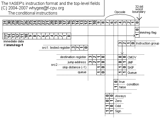
The YASEP (in 2007) provides 4 different conditional (and unconditional) groups of instructions, with different modes of operation :
On top of that, some instructions provide means to avoid a branch instruction :
The branches or skips can occur under some (homogenous) conditions, usually requiring the read of a register.
Except for the unconditional case, the conditions can be negated, so each group of conditional instructions has 1+(2×3)=7 sub-functions.
The YASEP can address 256MiB of memory.
The main reason comes from the 4 MSB of the data pointers that hold the auto-update flag. 32 bits - 4 = 28 bits for the addresses. This is well enough for embedded devices.
Programming with this processor requires a lot of caution to avoid accidental change of the uptade flags. Alterations of the 4 MSB as the result of additions (for example) could trap the processor to signal a pointer overflow. This can also occur when auto-inc/decrement wraps around (but then, only 28-bit address calculations are performed).
These 4 bits are less used in the instruction pointer, but the 2 MSB store the CQ when a trap occurs. The processor can thus restart at the right address with the right CQ, and needs only to save/restore 10 others registers (9 if it is smart) :
| Context buffer | ||
| Pos. | Data | Description |
| 0 | CQ|IP | Address of the instruction with the CQ |
| 1 | A(CQ+1) | |
| 2 | A(CQ+2) | |
| 3 | A(CQ+3) | |
| 4 | A4 | Queue #4's address register |
| 5 | A5 | Queue #5's address register |
| 6 | R0 | Standard register #0 |
| 7 | R1 | Standard register #1 |
| 8 | R2 | Standard register #2 |
| 9 | R3 | Standard register #3 |
So you see how fast context swap can be : because a queue's data just comes out of the memory, there is no need to save it. Only the pointer has to be saved, sparing six items from being transfered :-)
The catch is that the position of the 3 other queue numbers must be deduced from the indicated CQ, otherwise it would need 11 elements instead of 10. Well, that's just a few logic gates.
I have not yet determined how the address computations are performed. That might be inside or outside the execution core. Every cycle can perform 4 memory accesses (3 reads and 1 write, including instruction fetch) but 3 pointer updates (convention says that write has precedence over read for pointer updates). This means that 3 26-bit adders are needed in parallel with the core.
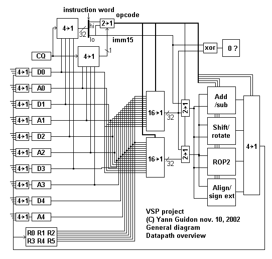
For ease of design, I have split the core into four stages as shown below :

This does not mean however that the core is pipelinable, despite some potential. It's not even worth considering this because it would bring little performance boost (50% ?) at the price of a lot of circuitry. The core works well, slowly but simply, without pipeline gates (here, the registers act as clock boundaries).
However, there might be another possibility later : transforming it into a SMT core (Simultaneous MultiThreading) to execute 2 or 4 threads, or more, concurrently. There, all the latencies are hidden from each others and interrupt latency might be greatly reduced. There is relatively few hazards to checks and the performance boost is much better than when simply pipelining. Each threads runs as slowly as in a Single-thread processor, but four threads would be able to run at the same time, boosting the instuctions per second rating. The only practical limitation would be the memory bandwidth, and some 32KB of onchip cache or SRAM would be helpful.
But that's for waaayyy later.
Now, you are encouraged to read the instruction set overview.
More informations (old, preliminary and written differently) can be found in this text