The microYASEP is a minimalistic subset of the YASEP family that targets microcontroller applications. It is optimised for size and should fit in a small FPGA, replacing monolithic microcontrollers that often don't have the required pins, peripherals or speed. The FPGA would handle high-speed signals in real time while the YASEP manages the system in the background. Since the microcontroller is integrated in the FPGA, cost and board space are reduced and the YASEP can be tailored exactly to the application, with even less communication issues: internal signals can be read and controlled directly by Special Registers or even normal registers.
Some of the constraints are :There is a little bonus however : in some versions, the condition codes can select one I/O pin among 16 (more than the RCA1802 ;-D).
Like many microcontrollers, the microYASEP has split memories, with one bank for data and another for instructions. Unified memory is possible but it depends on the available electronic circuits (multiport memories ?).
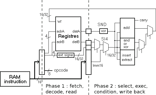
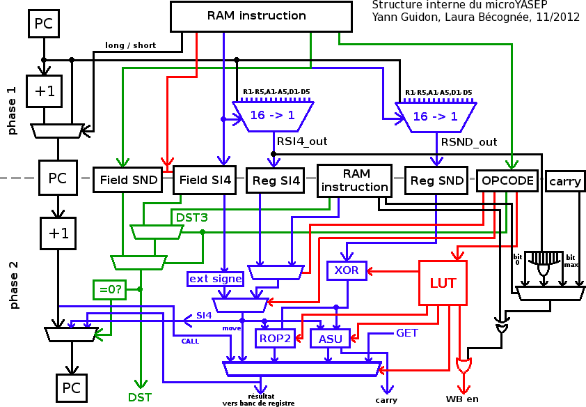
The instruction memory is 16-bits wide and provides one half-word at each clock cycle. Since the instructions have one or two half-words, the microYASEP executes one instruction in a fixed 2-phases cycle (each taking one clock cycle). Whether the instructions are short or long, their format is designed to allow maximum reuse of the decoding logic,
The instruction memory's access time is expected to be almost instantaneous (a few nanoseconds, or a fraction of the clock cycle). There is no read pipeline and the jumps are immediate (requiring no "delay slot" or insertion of delay cycles).
The registers might be implemented in logic gates. This spares two of the few SRAM blocks, the FPGA can store more instructions or data onchip. The registers are probably slower than the instruction memory...
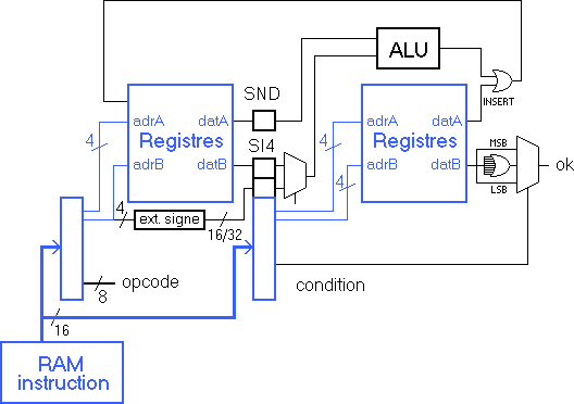
The register set is made of 16 registers, connected to the datapath by two big MUX that provide 2 data words per clock cycle. As there are two clock cycles for each instruction cycle, the microYASEP provides 4 operands per instruction: two of operations during the first phase, one condition and one additional data during the second phase.
The VHDL source code comprises about 360 lines. It is derived from the following diagram:
Legend (left to right):
The 16 bits version runs at approximately 20 MIPS on the A3P060 Flash-based FPGA.